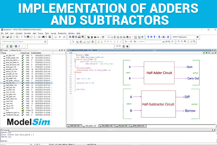
The moment we are asked to do big calculations, we reach out to the calculators to find the answers. But do we know how calculators perform the operations? The calculators have integrated chips that take care of the operations and give us the results. Adders and Subtractors are the basic elements of any ALU’s/Calculating Devices in this modern electronics world. In this tutorial, we are going to learn how to implement the Half adders, Full adders, Half Subtractors and Full Subtractors in VHDL using ModelSim.
This is a continuation of our sequence of tutorials, so if you are completely new to VHDL and Modelsim, please check out our VHDL tutorial series for more information on basics.
Half Adder in VHDL
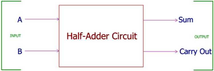
Half Adders' primary function is to add two bits or two digits, so the input port has two variables, A and B which corresponds to the digits/numbers that have to be added. The result of adding two bits/digits is the Sum and the Carryout which corresponds to the outputs ports. An example is shown below.
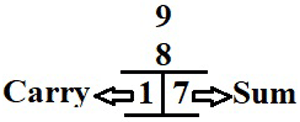
Here A=9, B=8, Sum=7, Carry Out=1. So, all these numbers that we enter in the calculators are converted into binary format and then the calculation is carried out. The Circuit Diagram of Half Adder and the Truth Table is given below.
|
A |
B |
Sum |
Carry Out |
|
0 |
0 |
0 |
0 |
|
0 |
1 |
1 |
0 |
|
1 |
0 |
1 |
0 |
|
1 |
1 |
1 |
1 |
From the Half Adder Truth Table, we can determine that A and B are the two bits that have to be added.
So, take a close look at the Sum column, it follows the XOR gate’s Truth Table and the Carry Out columns follows the AND gate’s Truth Table. The equation for the Sum and Carry Out is given below:
Sum<=A XOR B
Carry Out<= A AND B
The VHDL code for Half Adder is given below where the Data Flow Modelling is used as it involves only simpler equations.
library IEEE;
use IEEE.std_logic_1164.all;
entity half_adder is
port(A,B: in std_logic;
sum,carryout: out std_logic
);
end half_adder;
architecture flow of half_adder is
begin
sum<= A xor B;
carryout<=A and B;
end flow;
The libraries are declared, the entity is defined with the label “half_adder” and A, B, sum, carry_out as input and output ports, respectively. The architecture is defined with the two equations of sum <= A xor B and carryout<= A and B. So, this is a pretty simpler code where the equations of sum and carryout are defined.
Let's simulate this code by copying the code to the ModelSim. Refer to Implementation of Basic Logic Gates in VHDL for the steps involved in copying and simulation.
I have compiled the above code and simulated the same in ModelSim. The simulated waveform is given below:
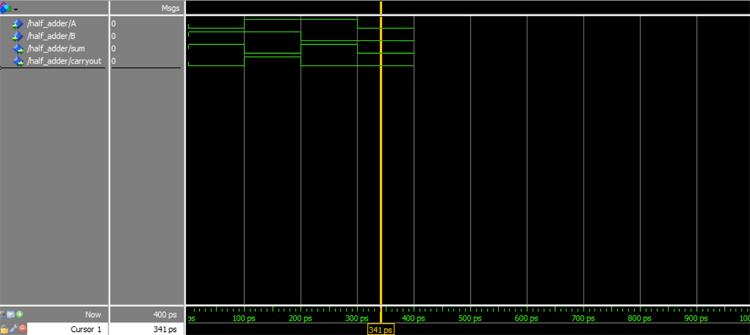
Move the cursor along the values 0-400ps to notice the change in the values of A, B, Sum, Carryout.
|
Timing(ps) |
A |
B |
Sum |
Carry Out |
|
0-100 |
0 |
1 |
1 |
0 |
|
100-200 |
1 |
1 |
0 |
1 |
|
200-300 |
1 |
0 |
1 |
0 |
|
300-400 |
0 |
0 |
0 |
0 |
We know how to implement half adders, let's now move on to the next segment, the Full Adders. In Full Adders, there in addition to the two input bits A and B, there is a carry-in bit. So, the full adders can be realized using 2 Half Adders and 1 OR Gate. The Full Adder Circuit Diagram is given below.
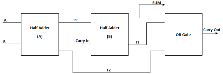
All the components are interconnected to design the Full Adder. Since these are interconnecting components, we can design using structural modelling. Refer to Designing of Boolean Logic-based IC to know how a circuit is designed using structural modelling. From the above figure, the variables T1, T2, T3 are the intermediary values that will be connecting the next component. The VHDL Code for Full Adder using structural modelling is given below.
VHDL Code for Full Adder:
library IEEE;
use IEEE.std_logic_1164.all;
entity full_adder is
port(A,B,carry_in: in std_logic;
sum,carry_out : out std_logic
);
end full_adder;
architecture flow of full_adder is
component half_adder is
port(A,B : in std_logic;
sum,carryout : out std_logic
);
end component;
component or_gate is
port(A,B : in std_logic;
Y : out std_logic
);
end component ;
signal T1,T2,T3:std_logic;
begin
half_adder1: half_adder port map (A=>A,B=>B,sum=>T1,carryout=>T2);
half_adder2: half_adder port map(A=>T1,B=>carry_in,sum=>sum,carryout=>T3);
or_gate1: or_gate port map(A=>T3,B=>T2,Y=>carry_out);
end flow;
Let's break the above code for better understanding. First, the libraries are imported as usual and the entity is declared with the label “full_adder” and the Inputs A, B, and Outputs sum, carry_out are declared.
library IEEE;
use IEEE.std_logic_1164.all;
entity full_adder is
port(A,B,carry_in: in std_logic;
sum,carry_out : out std_logic
);
end full_adder;
Next, the architecture is defined and the sub-components are defined. Here, the sub-components that are used are half-adder and OR gate. In general, the subcomponents are defined by “component label”. So here, “component half_adder” and “component or_gate” are the sub-components.
Note: Before scripting the VHDL code for Full adder, make sure to successfully compile the sub-components half adder and OR gate. The half adder code is given above and for VHDL OR gate code, you can refer using the link.
architecture flow of full_adder is
component half_adder is
port(A,B : in std_logic;
sum,carryout : out std_logic
);
end component;
component or_gate is
port(A,B : in std_logic;
Y : out std_logic
);
The next task is to interconnect the two half adders and the OR gate. Refer to the diagram given above. The intermediary values T1, T2, T3 are declared first.
signal T1,T2,T3:std_logic;
We are almost done with the last segment of the code. The components are interconnected with corresponding signal values. “half_adder1” and “half_adder2” is the respective label names for the half adders. So, the signals pass through the 2 half adders and the OR gate which is labelled as “or_gate1”.
begin
half_adder1: half_adder port map (A=>A,B=>B,sum=>T1,carryout=>T2);
half_adder2: half_adder port map(A=>T1,B=>carry_in,sum=>sum,carryout=>T3);
or_gate1: or_gate port map(A=>T3,B=>T2,Y=>carry_out);
end flow;
Just copy paste or type the above code in ModelSim and try simulating it. The simulation results for the above-given code are as follows.
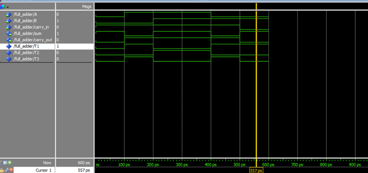
Scroll the cursor along the waveform to notice the change in values of the signal which corresponds to sum and carryout.
|
Timing(0-600 ps) |
A |
B |
Carry in |
Sum |
Carryout |
|
0-100 |
0 |
0 |
1 |
1 |
0 |
|
100-200 |
1 |
0 |
1 |
0 |
1 |
|
200-300 |
1 |
1 |
1 |
1 |
0 |
|
300-400 |
1 |
1 |
1 |
1 |
0 |
|
400-500 |
0 |
1 |
1 |
0 |
1 |
|
500-600 |
0 |
1 |
0 |
1 |
0 |
So, now that we know how to implement adders, we shall see how to implement subtractors.
There is no significant change in the structure of the VHDL code for subtractors when compared to the adders. The only change is in the difference and borrow. Take a look at Half Subtractors and Full Subtractors to know the basics.
Half Subtractor in VHDL: The circuit diagram for Half Subtractor and the expression for Difference and Borrow is given below for your reference.
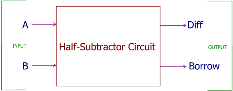
Difference<= A xor B;
Borrow<= AND B;
Here A' represents NOT of A.
VHDL code for Half Subtractor:
library IEEE;
use IEEE.std_logic_1164.all;
entity half_sub is
port(A,B: in std_logic;
diff,borrow : out std_logic
);
end half_sub;
architecture flow of half_sub is
begin
diff<= A xor B;
borrow<=not(A) and B;
end flow;
It's almost similar to the code of Half adder except for the fact that there is a change in the borrow equation. Just paste this code in ModelSim and you can obtain the results as shown below:
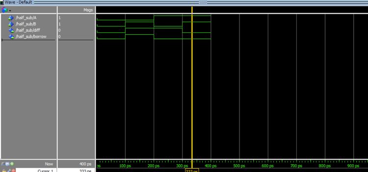
|
Timing(0-400 ps) |
A |
B |
Difference |
Borrow |
|
0-100 |
0 |
0 |
0 |
0 |
|
100-200 |
0 |
1 |
1 |
1 |
|
200-300 |
1 |
0 |
1 |
0 |
|
300-400 |
1 |
1 |
0 |
0 |
Full Subtractor in VHDL: Similar to Full Adder, full subtractor will have a third input as Borrow In. The circuit diagram is given below:

This is the same Structural modelling I used to design the Full Subtractor. T1,T2,T3 are the intermediary outputs. Here, the sub-components are 2 Half Adders and 1 OR gate. The VHDL code for Full Subtractor is given below.
library IEEE;
use IEEE.std_logic_1164.all;
entity full_sub is
port(A,B,borrow_in: in std_logic;
diff,borrow_out : out std_logic
);
end full_sub;
architecture flow of full_sub is
component half_sub is
port(A,B : in std_logic;
diff,borrow : out std_logic
);
end component;
component or_gate is
port(A,B : in std_logic;
Y : out std_logic
);
end component ;
signal T1,T2,T3:std_logic;
begin
half_sub1: half_sub port map (A=>A,B=>B,diff=>T1,borrow=>T2);
half_sub2: half_sub port map(A=>T1,B=>borrow_in,diff=>diff,borrow=>T3);
or_gate1: or_gate port map(A=>T3,B=>T2,Y=>borrow_out);
end flow;
Simulate the above-given code and we can obtain the results for a full subtractor circuit as given below.
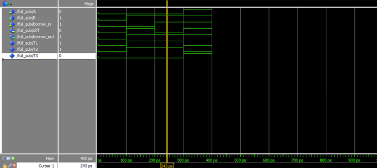
|
Timing(0-400 ps) |
A |
B |
Borrow In |
Difference |
Borrow Out |
|
0-100 |
0 |
0 |
0 |
0 |
0 |
|
100-200 |
0 |
1 |
0 |
1 |
1 |
|
200-300 |
0 |
1 |
1 |
0 |
1 |
|
300-400 |
1 |
1 |
1 |
1 |
1 |
Hence, Half Adder, Full Adder, Half Subtractor, and Full Subtractors are implemented using VHDL.
Complete Project Code
Half Adder:
library IEEE;

use IEEE.std_logic_1164.all;

entity half_adder is

    port(A,B: in std_logic;

         sum,carryout : out std_logic

);

end half_adder;

architecture flow of half_adder is

begin

sum<= A xor B;

carryout<=A and B;

end flow;
Full Adder:
library IEEE;

use IEEE.std_logic_1164.all;

entity full_adder is

    port(A,B,carry_in: in std_logic;

         sum,carry_out : out std_logic

);

end full_adder;

architecture flow of full_adder is

component half_adder is

    port(A,B : in std_logic;

         sum,carryout : out std_logic

);

end component;

component or_gate is

    port(A,B : in std_logic;

         Y : out std_logic

);

end component ;

signal T1,T2,T3:std_logic;

begin

half_adder1: half_adder port map (A=>A,B=>B,sum=>T1,carryout=>T2);

half_adder2: half_adder port map(A=>T1,B=>carry_in,sum=>sum,carryout=>T3);

or_gate1: or_gate port map(A=>T3,B=>T2,Y=>carry_out);

end flow;
Half Subtractor:
library IEEE;

use IEEE.std_logic_1164.all;

entity half_sub is

    port(A,B: in std_logic;

         diff,borrow : out std_logic

);

end half_sub;

architecture flow of half_sub is

begin

diff<= A xor B;

borrow<=not(A) and B;

end flow;
Full Subtractor:
library IEEE;

use IEEE.std_logic_1164.all;

entity full_sub is

    port(A,B,borrow_in: in std_logic;

         diff,borrow_out : out std_logic

);

end full_sub;

architecture flow of full_sub is

component half_sub is

    port(A,B : in std_logic;

         diff,borrow : out std_logic

);

end component;

component or_gate is

    port(A,B : in std_logic;

         Y : out std_logic

);

end component ;

signal T1,T2,T3:std_logic;

begin

half_sub1: half_sub port map (A=>A,B=>B,diff=>T1,borrow=>T2);

half_sub2: half_sub port map(A=>T1,B=>borrow_in,diff=>diff,borrow=>T3);

or_gate1: or_gate port map(A=>T3,B=>T2,Y=>borrow_out);

end flow;

